
- Turnkey Solution
- In order to achieve fast TAT for every step from prototype testing to mass production/supply, GAONCHIPS has established close partnerships with world-class foundries, package companies and test companies. We have completed many successful cases through our long-term strategic partnership program. We can provide total solution services from all steps (Package/Test/Q.A/Mass Production) of semiconductor process.
-
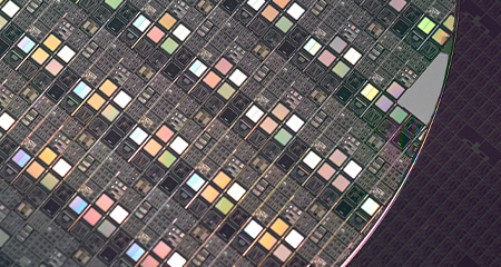
- Wafer Business
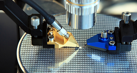
- Wafer fabrication without Wafer probing
-
- Known Good Die Business
- Wafer fabrication including Wafer probing
-

- Turnkey Business
- Complete all fabrication (Foundry / Package / Test)
-
01
Package Design Solution
-
Package bump / substrate Design
High-end design ( 2.5D PKG, Interposer design ) for AI Product
-
02
Package Validity check
-
Thermal Simulation / Thermal solution service
Electrical ( RLC, IR Drop, S-Parameter ) Simulation
Mechanical Simulation
-
03
Package Assembly solution
-
Assembly Process & condition setup
Parameter optimization ( DOE )
Clean BOM composition
-
01
Support for Test Solution
-
From IP Test Vector Provide to ATE Test setup
Corner Characteristics Analysis for mass productivity evaluation
-
02
Vector Conversion
-
Test Program Development
Load Board/Probe Card Design
-
03
Test Setup
-
Test Setup Interface with Test House
Test Vector Debugging Support
-
04
Mass Production Support
-
Low Yield Analysis
Product Characterization
Test Time Optimization
-
01
Customer Quality Service
-
Approval Documentation (PPAP etc.)
Customer Quality Issue handling
Automotive Service Pack solution
Customer Audit support
-
02
Product Qualification
-
Reliability Test based on AEC-Q100 or JEDEC
Manufacture Process qualification
Supplier Certification / Regular Audit
-
03
Quality Management
-
Quality management system by ISO compliance
Outsourcing quality control
Nonconforming Lot handling & monitoring
Failure Analysis for Customer return & Reliability failure
-
01
Signal Integrity
-
Signal Integrity by channel/Transient Simulation
Signal margin Assessment by EYE diagram based on JEDEC
Providing Solutions : Off-chip design ( PKG + Board ) Optimization
-
02
Power Integrity
-
Power Integrity by PDN ( Power Distribution Network ) Analysis
Power Noise Assessment based on JEDEC
Providing Solutions : DECAP budgeting to reduce power noise
-
01
Customer forecast management
-
02
Outsourcing Capacity control ( FAB, Package, Test )
-
03
Mass-Production control
-
Invoice, Build Instruction, WIP monitor
Wafer / Package / Test Yield control
-
04
Raw material Inventory control
-
Wafer, package substrate, EMC, packing material
-
05
Delivery control
-
TAT, Shipping, Logistic management