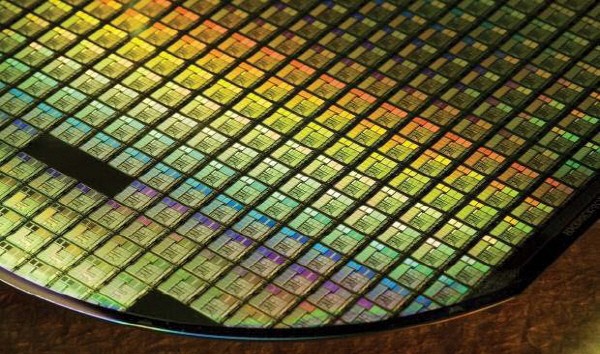
Hundreds of employees at the semiconductor design house
South Korean semiconductor design house companies have hired a large number of workers this year. Each company has secured additional manpower at least tens to as many as hundreds. As demand for ultra-fine processes under 14 nanometers of semiconductor fabless increased, the design house's "bulk up" move has accelerated to respond to it.

ADTechnology hired the most manpower among design houses. ADTechnology's executives and employees were less than 200 last year. This year, the workforce has expanded to 425. Considering its subsidiaries, there are more than 450 people. ADTechnology operates its U.S. and European branches to preparing for additional hiring.
SEMIFIVE has also expanded from 120 in 2020 to 190 this year. SEMIFIVE previously acquired design house Sesol Semiconductor and Dasim logic semiconductor designer. The company is expected to grow further as it is pursuing M&A another design house, HANATEC. HANATEC has about 60 people.
GAONCHIPS has also increased its workforce from about 100 to 150 this year. All of them are Samsung Electronics Foundry Design solution partners (DSP). Asicland is the only TSMC design partner in Korea and also hired 20 additional people this year.
The sharp increase in manpower is due to demand for advanced micro-processes. Recently, there have been more tasks (projects) for fabless domestic and foreign companies to design semiconductor chips with fine processes of 14 nanometers or less. Demand has increased especially in artificial intelligence (AI) and semiconductors for vehicles. AI semiconductor startups such as Furiosa AI, Rebellions, and Mobilint are designing chips with 5-14 nano processes. Telechips, which commercialized vehicle application processors (APs) with a 14-nano process, is also designing semiconductors for vehicles with an 8-nano process.

Semiconductor design has a significant increase in design support personnel as it goes into fine processes. This is because semiconductor integration increases. As the number of tasks to draw circuits in semiconductors increases significantly, a lot of design personnel are needed., CEO of ADTechnology, Joon-kyu Park said, "If we go to the 5-nano process, we need up to 50 to 100 people per task," and explained, "We need to deploy design support personnel on a large scale as the process becomes finer."
It was difficult to support the design of advanced processes under 14 nanometers with the size of existing design houses. Accordingly, the design house has grown its physique by aggressive M&A and hiring additional personnel. An official from Gaonchips said, "We have hired manpower and are currently training in preparation for micro-process tasks that will begin in earnest next year."
As Samsung Electronics and TSMC begin mass production of 3-nano processes next year, the size of the design house is expected to expand further. In the future, if domestic fabless also has the capability to utilize the 3-nano process, it is expected that the number of design house manpower will be expanded to support it.
| Company | 2020Y | 2021Y |
| ADTECHNOLOGY | 175 | 425 |
| SEMIFIVE | 120 | 190 |
| GAONCHIPS | 97 | 148 |
| ASICLAND | 81 | 100 |
By Staff Reporter Dong-jun Kwon (djkwon@etnews.com)
Hundreds of employees at the semiconductor design house - ETNews

